What Happens Inside a Chip Fab Cleanroom That Marketing Photos Never Show

Wei Zhang
July 9, 2026
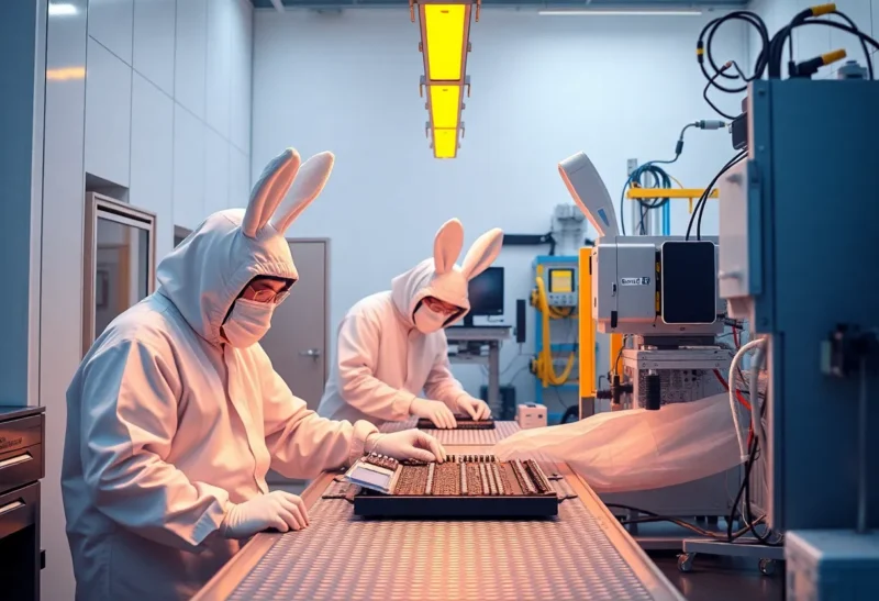
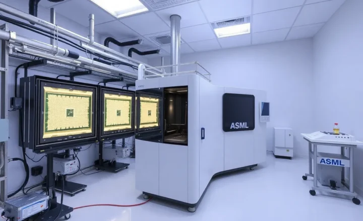
Every semiconductor company’s promotional material eventually includes the same shot: rows of workers in full white “bunny suits,” bathed in yellow light, standing beside gleaming equipment in an impossibly clean-looking room. It’s a genuinely accurate image as far as it goes, but it also flattens one of the most demanding manufacturing environments in existence into something that looks almost sterile and simple. I’ve spent years working as a semiconductor engineer around fab operations, and the actual operational reality inside a cleanroom — the contamination control obsession, the yellow lighting’s real purpose, and just how much of the work happens without any human presence at all — is considerably stranger and more exacting than the marketing photos convey.
Why “Clean” Doesn’t Mean What You’d Assume
A modern leading-edge fab cleanroom is classified at ISO Class 1 or better under the international cleanroom standard, meaning fewer than 10 particles larger than 0.1 micrometers per cubic meter of air — for comparison, a typical hospital operating room, itself considered an exceptionally clean environment, runs at roughly ISO Class 5 to 7, meaning it contains thousands of times more airborne particles than a leading-edge fab floor. This level of particle control matters because modern transistor features are now measured in single-digit nanometers, small enough that even one stray dust particle landing on a wafer during a critical process step can create a defect that ruins that specific location on the chip, and at these feature sizes, particles far too small to see with the naked eye, or even with most conventional microscopy, are large enough to be catastrophic to a chip’s function.
Achieving this requires continuous, massive air filtration — fab cleanrooms typically replace their entire air volume with freshly HEPA and ULPA-filtered air dozens of times per hour, using raised floor and ceiling designs that allow air to flow in a continuous, unidirectional downward pattern (called laminar flow) specifically to sweep any particles that do get generated straight down and out through the perforated floor before they can settle on exposed wafers, rather than allowing them to circulate and settle randomly the way air does in an ordinary room.
What the Yellow Light Actually Does
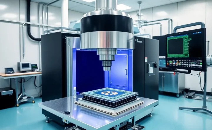
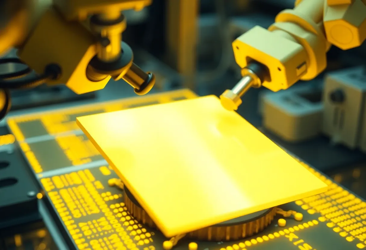
The yellow lighting that’s become such a visually distinctive feature of cleanroom photography isn’t an aesthetic choice — it’s a functional necessity tied directly to the photolithography process, the step where a chip’s circuit patterns are actually transferred onto a wafer’s photosensitive coating (called photoresist) using precisely controlled light exposure. Photoresist material is specifically formulated to be sensitive primarily to short-wavelength UV and blue light, the wavelengths actually used in the lithography exposure process itself, and any incidental exposure to those wavelengths from ordinary ambient room lighting could partially and unpredictably expose photoresist before it’s supposed to be exposed, ruining the precision of the intended pattern.
Standard fab lighting filters out these shorter wavelengths, leaving only longer wavelength yellow-amber light that photoresist isn’t sensitive to, which is why cleanroom photolithography bays specifically (not necessarily every area of a fab) are lit in that distinctive yellow glow — a direct, functional solution to a specific chemical sensitivity problem, not a stylistic or safety-related lighting choice as the marketing imagery sometimes implies without explanation.
Why Humans Are Actually the Biggest Contamination Risk
The full-body bunny suits, which cover essentially every part of a worker’s body including hair, face (through a filtered mask or hood), and skin, exist because human bodies are, by a wide margin, the largest source of particle contamination cleanroom protocols have to actively manage — ordinary skin shedding, hair, clothing fiber, and even exhaled breath all introduce particle counts that would overwhelm cleanroom particle limits almost immediately without this level of containment. Workers go through a multi-stage gowning process before entering the cleanroom floor, including air showers designed to blow off any loose particles clinging to the suit’s exterior before the worker proceeds further into the facility, and strict protocols govern what can and can’t be brought onto the floor, since even paper, certain fabrics, and standard cosmetics can shed particles at rates incompatible with cleanroom contamination limits.
This human contamination risk is a major reason why modern leading-edge fabs have moved toward minimizing direct human presence on the cleanroom floor wherever technically possible, relying instead on automated wafer handling systems — enclosed transport pods called FOUPs (Front Opening Unified Pods) move wafers between process tools via overhead automated rail systems or floor-based robotic transport, keeping wafers in a sealed, filtered micro-environment even while moving between different processing stations, rather than exposing them to the broader cleanroom’s ambient particle count during transport, which even at ISO Class 1 levels still carries meaningfully more particle risk than a wafer sealed inside its own dedicated FOUP enclosure.
The Vibration and Temperature Control Nobody Mentions
Contamination control gets most of the public attention, but leading-edge fabs manage an equally demanding set of environmental controls that rarely make it into promotional materials at all: vibration isolation and temperature stability. Modern lithography tools position features with sub-nanometer precision, meaning even minor building vibration — from nearby equipment, foot traffic, or external sources like passing vehicles or construction — can introduce positioning errors that degrade pattern accuracy, which is why fab buildings are typically constructed with massive isolated foundation slabs and vibration-dampening structural design specifically to keep floor-level vibration within tolerances that would seem excessive for almost any other kind of industrial building.
Temperature stability requirements are similarly extreme — many critical process areas maintain temperature control within a fraction of a degree Celsius continuously, because thermal expansion and contraction of both the equipment and the wafers themselves, even at very small magnitudes, can measurably affect pattern alignment accuracy at these feature sizes, requiring HVAC systems engineered to a level of precision and redundancy considerably beyond what almost any other manufacturing environment requires simply to keep the physical process capable of the accuracy leading-edge chip production demands.

Why This Level of Control Costs What It Does
Building and operating a leading-edge fab cleanroom to these standards is a substantial part of why modern fab construction costs have climbed into the tens of billions of dollars for a single facility — TSMC’s and Intel’s most advanced facilities represent some of the most capital-intensive single manufacturing sites ever built, and cleanroom infrastructure, environmental control systems, and automated material handling represent a genuinely large share of that total cost, not merely the specialized lithography and etching tools that typically get more attention in cost breakdowns.
This cost structure is also a major reason why leading-edge chip manufacturing has consolidated into such a small number of companies globally capable of operating at this level — TSMC, Samsung, and Intel represent nearly all current leading-edge logic manufacturing capacity — because the combination of contamination control, vibration isolation, and automated handling infrastructure required to run a modern fab at competitive yield represents an engineering and capital barrier that few organizations in the world can realistically clear, a genuinely underappreciated part of why the semiconductor industry’s geographic and corporate concentration has become such a significant policy and supply chain concern in recent years.