How Lithography Works and Why It Determines the Future of Chip Performance

Helena Voss
July 7, 2026
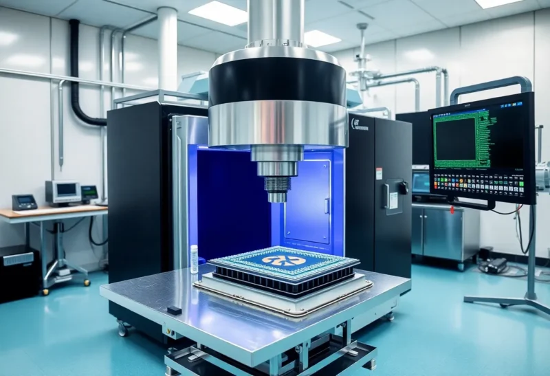
Semiconductor manufacturing is a discipline that produces the most complex objects humans have ever made, and lithography is the step in that process that determines what’s possible. Every processor, memory chip, and graphics chip in production today depends on lithography to define the circuits that make it function, and the limits of lithography directly set the limits of what can be built on a chip. Understanding how lithography works explains why TSMC, Samsung, and Intel pursue EUV (Extreme Ultraviolet) light sources, why the smallest transistors in production are measured in angstroms, and why the geopolitics of semiconductor manufacturing are so concentrated around a small number of specialized companies.
The Basic Principle: Printing Patterns With Light
Semiconductor lithography is essentially a photographic process. The fundamental operation: coat a silicon wafer with a light-sensitive material (photoresist), expose it to light through a mask (a patterned template defining the circuit), and then develop the exposed photoresist, removing either the exposed or unexposed regions depending on the resist type. The remaining photoresist protects some areas of the silicon while the unprotected areas are etched or implanted with dopants to create the transistor structures and interconnects that make up a chip.
The key physical constraint is that light cannot resolve features smaller than approximately half its wavelength. This is the Rayleigh criterion: the theoretical minimum feature size resolvable by an optical system is proportional to the wavelength of light used. Visible light at 400–700nm could never produce the sub-10nm features in modern chips. The relentless pressure to shrink features — Moore’s Law’s continuous density improvement — required relentlessly shortening the wavelength of light used in lithography.
The progression: early semiconductor manufacturing used mercury arc lamp wavelengths (436nm, 365nm); the industry moved to deep ultraviolet (DUV) at 248nm (krypton fluoride laser) and then 193nm (argon fluoride laser). These wavelengths produce features in the 90nm–28nm range. Below 28nm, the industry ran into the fundamental limits of 193nm light for single-exposure patterning and developed immersion lithography (replacing air with water between the lens and wafer, increasing the effective numerical aperture and improving resolution) and then multi-patterning techniques to use 193nm wavelength for features smaller than its theoretical single-exposure limit.
EUV: The Current Frontier
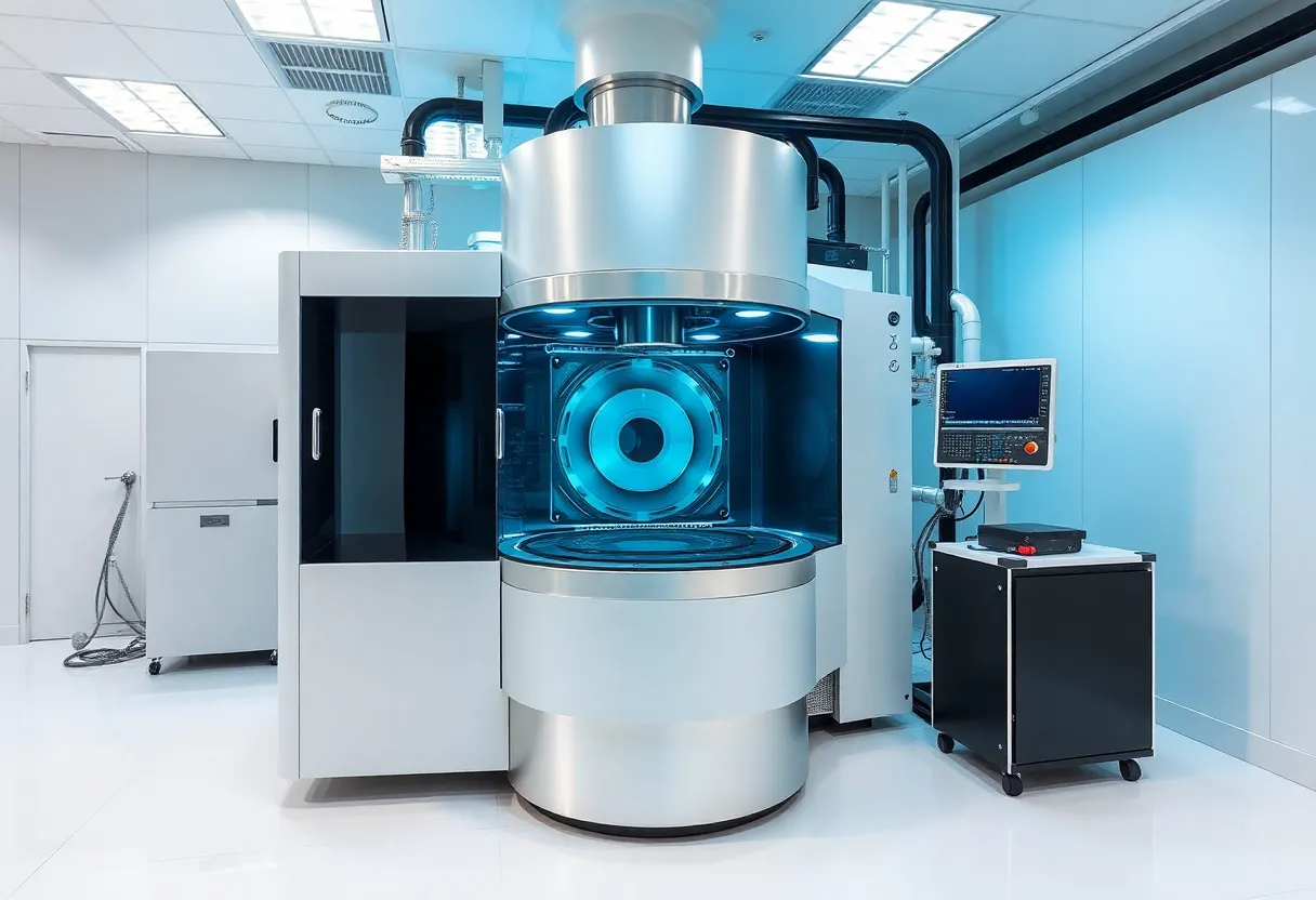
Extreme Ultraviolet (EUV) lithography uses 13.5nm wavelength light — nearly X-ray rather than ultraviolet — which allows direct patterning of features at the scale required for 5nm, 3nm, and below process nodes without the complex multi-patterning required for DUV at these scales. EUV was in development for decades before reaching production: the technical challenges were enormous.
EUV light at 13.5nm is absorbed by essentially everything, including air and any transmissive optical material — it cannot use lenses made from glass as conventional optics do, because glass absorbs EUV. EUV optics are entirely reflective: the light bounces off a series of precisely curved multilayer mirrors rather than passing through lenses. The entire optical path must be kept in vacuum because even air absorbs EUV significantly. The light source — created by focusing a high-power CO2 laser onto a stream of tin droplets that vaporize into plasma emitting at 13.5nm — is extraordinarily complex and is the primary engineering challenge that kept EUV from production for many years.
ASML, the Dutch company that manufactures EUV lithography machines, is the only company in the world that produces them. An EUV machine costs approximately $200 million and takes years to manufacture, assembling components from hundreds of suppliers with tolerances measured in nanometers. The mirrors alone — polished to within a fraction of a nanometer of their theoretical shape — represent a manufacturing achievement without precedent. ASML’s dominance of this market is a function of the extraordinary difficulty of what their machines do: no other company has successfully built an EUV machine for production use.
High-NA EUV: The Next Step
The current generation of EUV machines (“Low-NA” EUV with numerical aperture of 0.33) produces patterns at the 3nm process node and is being pushed toward 2nm. The next generation — High-NA EUV machines with numerical aperture of 0.55 — increases resolving power further, enabling patterns at 2nm and below nodes. ASML has begun delivering High-NA EUV machines to Intel (which has been their first major customer for this technology, part of Intel’s aggressive push to reclaim process node leadership) and is developing production capacity for TSMC and Samsung adoption.
High-NA EUV is more complex than Low-NA: the larger numerical aperture requires physically larger mirrors and a different optical architecture, and the depth of focus decreases (meaning the wafer must be flatter and the process more tightly controlled). The machines cost over $350 million each. The pace of investment required to advance lithography at each generation is part of why semiconductor manufacturing has become increasingly concentrated among three companies (TSMC, Samsung, Intel Foundry) that can amortize billions in R&D and equipment costs across large production volumes.
Why This Determines Chip Performance
Transistor size affects three interconnected properties: switching speed, power consumption, and density. Smaller transistors switch faster and use less power, and higher density means more transistors per unit area — more compute capability in the same physical space. The link between process node and performance is why every major chip announcement leads with the process node: TSMC N3 (3nm), N2 (2nm); Samsung’s SF3; Intel’s Intel 18A. These numbers are not strictly the physical dimensions of the smallest features (the “nm” nomenclature has become a marketing label with variable relationship to physical dimensions), but they represent real improvements in transistor density and efficiency at each generation.
The limits of lithography set the limits of what’s achievable at each process node. Beyond the physical lithography limit, 3D stacking — stacking multiple chip layers vertically — provides density improvements without requiring smaller 2D features. Intel’s Foveros, TSMC’s SoIC, and various hybrid bonding technologies increasingly allow chipmakers to achieve system-level density improvements beyond what planar lithography can deliver alone. The future of chip scaling is increasingly three-dimensional, but lithography advancement remains the enabling technology that determines what each layer of those stacked structures can contain.