How Semiconductor Packaging Has Become as Important as the Chip Itself

Wei Zhang
July 7, 2026
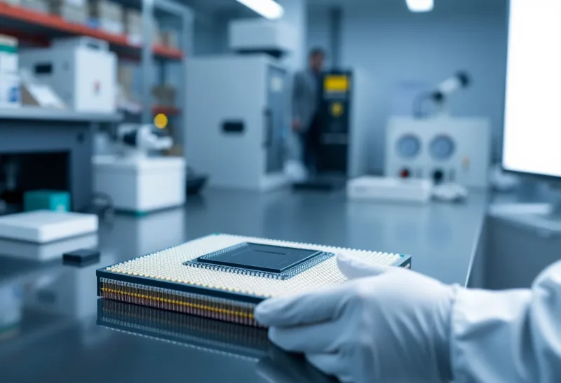
For most of semiconductor history, chip performance was primarily a function of what happened inside the chip—transistor density, process node, architecture. Packaging was the relatively unglamorous step at the end of the manufacturing process: encase the chip in a protective housing, add the electrical connections that allowed it to plug into a circuit board, and ship it. Advanced packaging was a niche concern for high-performance applications that needed better heat dissipation or smaller form factors.
That hierarchy has inverted. As transistor scaling has slowed—moving from 7nm to 5nm to 3nm still happens but at longer intervals, higher costs, and with diminishing returns—the industry has increasingly turned to packaging innovations to achieve the performance improvements that process scaling alone can no longer deliver. The result is that semiconductor packaging has become a primary engineering frontier, with techniques like chiplets, 2.5D integration, 3D stacking, and advanced interconnects delivering performance gains that would have required another process node a decade ago.
Why Scaling Alone Is No Longer Enough
Moore’s Law—the observation that transistor density roughly doubles every two years—has slowed significantly from its historical pace. The physical, engineering, and economic barriers to scaling transistors below 3nm are substantial: quantum tunnelling limits how thin gate oxides can be, extreme ultraviolet (EUV) lithography equipment costs hundreds of millions of dollars per tool, and the engineering complexity of designing chips at leading nodes has grown faster than the performance benefits.
The practical consequence for chip designers is that the performance improvement from moving to the next process node is smaller and more expensive than it was historically. A 5nm chip is not dramatically faster than a 7nm chip on a per-clock basis—the improvement comes primarily from reduced power consumption at equivalent clock speeds, which enables more transistors in the same thermal budget. The era of straightforward performance scaling from process node advancement is over.
Packaging innovations offer a different lever: instead of making individual transistors smaller, you can arrange multiple chips in ways that improve their collective performance—connecting them with shorter, faster, lower-power interconnects than a conventional PCB provides, stacking memory directly on top of processors to eliminate the memory bandwidth bottleneck, or combining different specialised chips from different process nodes into a single high-performance package.
Chiplets: Modularity Over Monolithic Design
The chiplet approach represents one of the most significant architectural shifts in semiconductor design in decades. Rather than designing a single monolithic die that includes all the required logic and memory, chiplet designs separate the chip into multiple smaller dies (chiplets) that are assembled together in the package.
AMD’s EPYC server processors are the clearest example: instead of a single large die with all CPU cores, the design uses multiple CPU core dies (the “Core Complex Dies” or CCDs) connected to I/O dies through high-bandwidth interconnects on an organic substrate or silicon interposer. The advantages are significant: smaller dies have higher yields (fewer defects affect any given die), different functional blocks can be manufactured on different process nodes (CPU cores on the most advanced node, I/O on a mature node), and the modular approach allows faster product differentiation (different core counts from the same CCD building blocks).
Intel’s Foveros technology and Apple’s M-series UltraFusion packaging use 3D and 2.5D chiplet integration respectively. The Nvidia H100 AI accelerator uses high-bandwidth memory (HBM) stacked alongside the GPU die on a silicon interposer—a 2.5D configuration that provides the memory bandwidth essential for large language model inference and training at performance levels impossible with conventional GDDR memory on a PCB.
2.5D and 3D Integration: The Interconnect Revolution
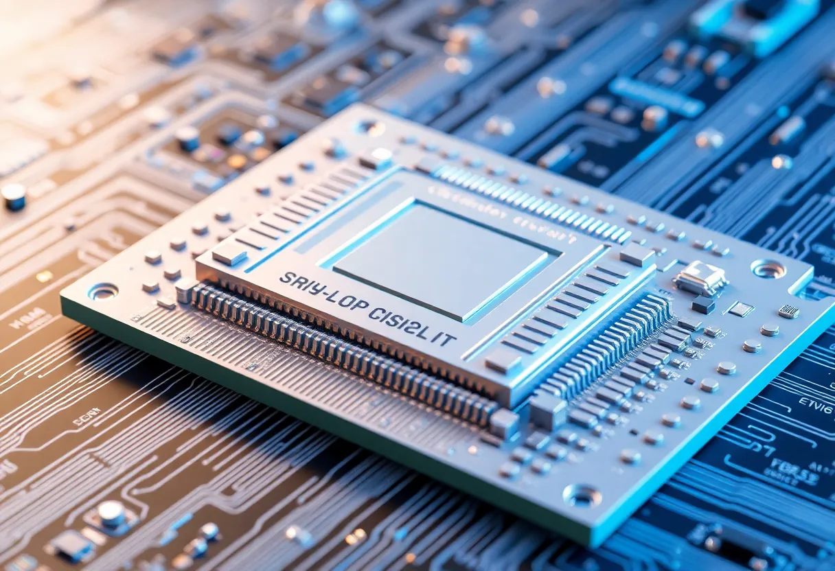
The terms 2.5D and 3D refer to how chips are physically arranged in the package. In conventional 2D packaging, all dies sit on the same plane. 2.5D integration uses a silicon interposer—a thin silicon substrate with extremely fine interconnect traces—to connect multiple dies side by side with interconnect densities far exceeding what a conventional PCB or organic substrate can achieve. 3D integration stacks dies vertically, connecting them through the die substrate using Through-Silicon Vias (TSVs).
The performance advantage of these interconnects is fundamental: electrical signals travel faster, at lower power, over shorter distances. The latency and bandwidth of a memory interface depends critically on the physical distance between the processor and memory. Connecting HBM memory to a GPU via a silicon interposer achieves interconnect bandwidths of hundreds of GB/s that would be physically impossible with conventional PCB routing.
TSMC’s Chip-on-Wafer-on-Substrate (CoWoS) and System-on-Integrated-Chips (SoIC) technologies, Intel’s EMIB (Embedded Multi-die Interconnect Bridge) and Foveros, and Samsung’s X-Cube are the primary advanced packaging platforms from the major semiconductor manufacturers. These technologies require engineering investment and manufacturing sophistication comparable to the process node itself—the distinction between “packaging” and “manufacturing” is becoming blurred.
Memory Bandwidth: The Bottleneck That Packaging Addresses
The performance of many modern compute workloads—AI inference and training, high-performance computing, video processing—is limited not by processor speed but by memory bandwidth: the rate at which data can be moved between memory and compute. Conventional DRAM connected to a processor via a PCB provides bandwidth limited by the number and speed of physical pins, constrained by signal integrity at high frequencies over relatively long PCB traces.
High Bandwidth Memory (HBM) technology stacks multiple DRAM dies vertically and connects them through TSVs to produce memory modules with dramatically higher bandwidth than conventional GDDR: HBM3 provides over 665 GB/s per stack versus approximately 80 GB/s for GDDR6X at similar power. The higher bandwidth is achievable because the wide parallel interface enabled by TSV interconnects replaces the limited pin-count interfaces that PCB routing constrains.
The memory bandwidth improvement is the primary reason that AI accelerators like the Nvidia H100 and AMD MI300 series can process the large model weights and activations of today’s large language models at practical speed. Without advanced packaging enabling HBM integration, the compute capability of these chips would be largely bottlenecked by memory access rather than arithmetic throughput.
Advanced Packaging as a Competitive Moat
The manufacturing complexity of advanced packaging has created a competitive dynamic in the semiconductor industry that extends well beyond chip design. TSMC’s CoWoS capacity—which determines how many AI accelerators can be produced—became a significant bottleneck in 2023-2024 as demand for AI compute hardware surged, because CoWoS packaging capacity expanded more slowly than front-end wafer fabrication capacity.
The geopolitical dimension of advanced packaging is also significant. Advanced packaging for leading-edge chips is concentrated at TSMC and Samsung in Taiwan and South Korea, with limited capability in the US, Europe, and Japan—though the CHIPS Act investments and equivalent programmes in other regions are directing substantial funding toward building advanced packaging capacity in geographically diversified locations.
For chip designers, advanced packaging has shifted what’s possible at a given cost point. A chip designed to leverage chiplets and 2.5D HBM integration can achieve better performance per watt and performance per dollar than a comparable monolithic chip at the same or more advanced process node. This means that packaging architecture is now a primary design consideration from the beginning of the chip development process, not an afterthought at the end—and that the teams and companies with the most advanced packaging expertise have a meaningful competitive advantage in high-performance computing, AI, and networking applications.