The Engineering Behind Modern Lithography: How Chips Get Their Patterns

Wei Zhang
July 7, 2026
The transistors in a modern processor are measured in nanometers—billionths of a meter. The most advanced chips in production in 2026 have feature sizes around 2–3 nanometers in the marketing nomenclature, with actual physical transistor dimensions somewhat larger but still in single-digit nanometer territory. These structures are too small to see with a visible-light microscope. They’re smaller than the wavelength of the light used to create them, which seems like a contradiction until you understand how lithography actually works.
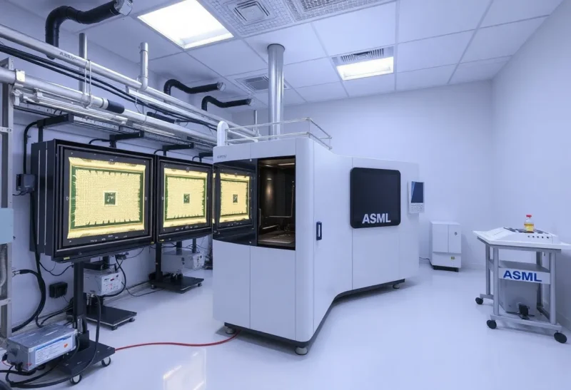
Semiconductor lithography—the process of printing circuit patterns onto silicon wafers—is one of the most complex manufacturing processes humans have ever developed. The machines that do it are among the most intricate and expensive industrial equipment ever built. ASML’s extreme ultraviolet lithography (EUV) machines, the most advanced in production, cost around $400 million each, weigh approximately 180 metric tons, and require years to order after placement. Understanding what they do and why it’s so difficult helps explain why advanced chip manufacturing is one of the most concentrated and hard-to-replicate capabilities in global industry.
The Basic Principle: Photolithography
Photolithography, at its core, is a sophisticated version of what darkroom photography does. A photosensitive material (photoresist) is coated onto a surface (the silicon wafer). Light is shone through a patterned mask (reticle) onto the photoresist. Where light hits, the photoresist changes chemically. When developed, the exposed or unexposed regions are removed, leaving a physical pattern. That pattern is then used in subsequent processing steps to etch, deposit, or implant materials into the silicon.
The pattern transferred defines where transistors, conductors, and insulators go. A modern chip requires dozens of patterning steps—each adding a layer of structure—before the final chip emerges. The smallest features that can be resolved depend fundamentally on the wavelength of light used, which determines the diffraction limit: features smaller than roughly half the wavelength can’t be cleanly resolved.
This relationship between wavelength and resolution drove semiconductor manufacturers to progressively shorter wavelengths over decades. Early photolithography used visible light (wavelengths around 400–700 nm). Then deep ultraviolet (DUV) at 248 nm using krypton fluoride excimer lasers. Then DUV at 193 nm using argon fluoride lasers, which became the workhorse of the industry for more than two decades.
Resolution Beyond the Wavelength: Immersion and Multiple Patterning
The 193 nm DUV wavelength imposes a fundamental limit on feature size, but the industry found ways to push below that limit without changing the light source.
Immersion lithography, introduced in the mid-2000s, fills the space between the final lens element and the wafer with highly purified water (refractive index ~1.44) instead of air. This effectively shortens the wavelength by the refractive index factor, giving an effective wavelength of about 134 nm. Immersion DUV became the standard and enabled feature sizes well below what dry 193 nm lithography could achieve.
Multiple patterning pushed further. By exposing and developing the same layer multiple times, with carefully aligned separate masks, features smaller than a single exposure’s resolution limit can be created through their interaction. Double patterning, triple patterning, quadruple patterning—the number of passes increased as manufacturers squeezed more resolution out of the 193 nm immersion system. This works, but it’s extremely expensive (each extra pass is a full photolithography cycle), precision-demanding (misalignment between passes degrades the pattern), and fundamentally limited in how far it can go.
EUV: The Wavelength That Solved Everything—At Enormous Cost
Extreme ultraviolet lithography uses 13.5 nm wavelength light—roughly 14 times shorter than the 193 nm DUV light it replaces. At 13.5 nm, you can directly resolve features that multiple patterning of 193 nm light could only laboriously approximate. One EUV exposure can replace several DUV patterning passes, reducing process complexity and potentially improving yield.
The problem is that 13.5 nm EUV light is absorbed by virtually everything—air, water, glass, almost all optical materials. This makes EUV engineering extraordinarily difficult.
The light source uses a laser to vaporize tiny tin droplets (around 50 microns in diameter) with an initial pulse to flatten and expand them, followed by a second, more powerful pulse to create a tin plasma. The tin plasma emits EUV light at 13.5 nm—the desired wavelength—among other wavelengths. The EUV light is separated from other emissions using spectral filters and collector mirrors.
Because glass lenses absorb EUV completely, the entire optical system uses mirrors—carefully shaped and coated with multilayer reflective stacks (typically alternating molybdenum and silicon layers) that reflect EUV while absorbing longer wavelengths. Each mirror reflects only about 70% of incident EUV; a system with multiple mirrors sees significant power loss at each reflection. The mirrors must be among the most precise optical surfaces ever manufactured—nanometer-scale surface accuracy across a surface that might be a meter in diameter.
The entire optical path must be maintained in vacuum—not just low pressure, but high vacuum—because EUV is absorbed by air. The full EUV system, from light source to wafer stage, operates in a vacuum environment that must be maintained without compromising the precision of all the moving components within it.
The wafer stage—the mechanism that moves the silicon wafer into position for each exposure—must position the wafer to within fractions of a nanometer while moving rapidly enough to maintain commercial throughput. Modern EUV systems can expose wafers at rates of around 150 wafers per hour, each wafer receiving dozens to hundreds of separate exposures aligned to each other with sub-nanometer precision.
High-NA EUV: The Next Step
Standard EUV machines use a numerical aperture (a measure of the light-gathering angle of the optical system) of 0.33. ASML and Intel are leading the deployment of High-NA EUV machines with a numerical aperture of 0.55—a 70% improvement that directly translates to finer resolution. High-NA EUV enables feature sizes around 2 nm and below in single exposures, removing the need for multiple patterning at these scales.
The first High-NA EUV machines entered production in 2024, with Intel being among the first to install them. These machines represent a further step in cost and complexity—even more expensive than standard EUV, requiring new process development, new photoresists, and new optical designs. Each installed machine represents years of engineering by ASML, Zeiss (which makes the optical systems), and multiple supply chain partners.
The Photoresist: Chemistry at the Edge of Resolution
The photoresist—the photosensitive material that records the light pattern—is a critical component of lithography that often gets less attention than the optical system. EUV photoresists must respond to photons at 13.5 nm wavelength and produce sharp, accurate pattern edges at the resolution required by modern process nodes. This is challenging because EUV photons are energetic enough to cause complex secondary electron cascades in the resist, and the stochastic (random) nature of photon absorption at very small feature sizes can cause local variations in resist exposure.
Metal oxide resists—materials incorporating metal atoms that interact strongly with EUV—have emerged as a category with better EUV absorption and potentially sharper pattern edges than traditional polymer chemists. The development of EUV-compatible photoresist chemistry is an active research area with direct implications for how well EUV lithography can resolve features at the most advanced nodes.
Why This Creates Concentration
The extreme difficulty of EUV technology explains why semiconductor lithography has concentrated to a remarkable degree. ASML is the world’s only manufacturer of EUV lithography machines—and has been for years. The company’s dominant position is not an accident but a result of the enormous technical and financial investment required to develop EUV. Competitors tried and withdrew.
The supply chain supporting EUV is similarly concentrated. Zeiss makes the optical systems. A handful of companies globally produce the tin droplets, the photoresists, and the multilayer mirror coatings. The raw materials—extremely high-purity silicon, specific rare metals for mirror coatings, specialized chemicals—come from a handful of specialized suppliers.
This concentration creates both geopolitical significance (EUV machines are subject to export controls restricting their sale to certain countries) and supply chain fragility. Disruptions anywhere in the ASML ecosystem have direct consequences for the global chip supply.
What Comes After EUV
The semiconductor industry’s roadmaps project continued scaling, but the physical path becomes harder at each step. Hyper-NA EUV—systems with numerical aperture above 0.55—is being discussed for nodes beyond what current High-NA machines can achieve. Alternative approaches like directed self-assembly (using materials that self-organize into regular patterns at small scales) and computational lithography (using advanced algorithms to compensate for optical imperfections) continue to be developed.
Moore’s Law—the observation that transistor density roughly doubles every two years—has slowed from its historical pace. The cost per transistor is no longer falling as quickly as it once did, and the engineering required to continue scaling has become qualitatively more difficult. EUV bought the industry another generation; what comes after High-NA EUV is not fully defined.
What is certain is that the ability to print features at nanometer scales—a capability that didn’t exist decades ago—is now foundational to modern civilization. Every smartphone, every data center, every medical device with a processor depends on lithography. The machines that do it are the most sophisticated manufacturing equipment humans have built, and they represent one of the most concentrated technological capabilities in global industry.