Why Perovskite Solar Cells Keep Missing Their Commercial Debut

Futurion Editorial
July 9, 2026
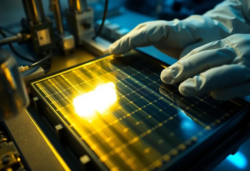
Every few months, a materials science lab announces a new record: a perovskite solar cell that converts more sunlight into electricity than anything silicon has managed in the lab. The efficiency numbers keep climbing past 26%, then 27%, edging toward theoretical limits that would have seemed absurd a decade ago. Headlines call it the technology that will finally dethrone silicon, the material that will make solar panels cheaper, lighter, and more efficient than anything on your neighbor’s roof today.
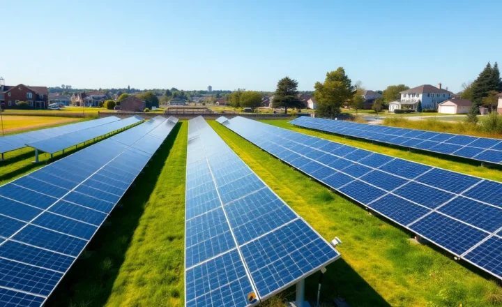
And yet, if you go shopping for solar panels this year, you will not find a single perovskite module for sale to homeowners. Not one. The technology that keeps breaking efficiency records in university labs and startup pilot lines has, for nearly fifteen years, failed to make the jump to your roof. That gap between laboratory promise and commercial reality is not an accident or a funding problem. It is a set of specific, stubborn engineering failures that keep resetting the clock on “five years away.”
A Material That Almost Seems Too Good
Perovskites are not a single substance but a crystal structure — named after the mineral perovskite, first described in the Ural Mountains in 1839 — that a huge range of compounds can adopt. The versions used in solar cells are typically hybrid organic-inorganic halides, often built around lead, iodine, and a small organic cation. What makes them exciting is how they are made: instead of growing silicon crystals in furnaces at over 1,400°C and slicing them into wafers, perovskite films can be deposited from a liquid solution at room temperature, essentially printed onto glass or flexible plastic like ink.
That single difference changes the economics of the entire industry. Silicon photovoltaic manufacturing is capital-intensive, energy-hungry, and slow to retool. Perovskite deposition, in principle, could be done with equipment resembling a large inkjet printer, at a fraction of the energy cost and on flexible substrates that silicon can never use. Combine that with efficiency numbers that already rival or beat commercial silicon, and it is easy to see why so much venture capital and government research money has poured into the field since Japanese researcher Tsutomu Miyasaka’s group first reported a working perovskite solar cell in 2009.
The efficiency trajectory has been genuinely remarkable. Silicon took roughly forty years to climb from lab curiosity to its current commercial efficiency ceiling. Perovskites covered a comparable distance in efficiency gains in under a decade. Tandem cells — where a perovskite layer sits on top of a silicon cell, each absorbing a different part of the solar spectrum — have pushed past 33% efficiency in lab settings, a number silicon alone will likely never reach because of fundamental physical limits tied to its bandgap.
The Problem Nobody Wants to Put on a Press Release
Here is the number that matters more than any efficiency record: a rooftop solar installation is expected to keep producing power reliably for 25 to 30 years. Silicon panels routinely meet that bar, degrading by less than half a percent per year under normal conditions. Perovskite cells, despite years of intensive engineering, still cannot make that promise with a straight face.
The core issue is that the same ionic, soft crystal structure that makes perovskites easy to process from solution also makes them chemically unstable. Moisture is the most obvious enemy — even trace humidity can begin breaking down the crystal lattice within weeks in early formulations, turning the vivid black active layer visibly yellow as it decomposes into lead iodide and other breakdown products. Heat is another problem: the same afternoon sun the panel is supposed to be harvesting can push cell temperatures past 60°C, and many perovskite formulations show accelerated degradation right in that operating range. UV exposure, oxygen, and even the electrical bias applied during normal operation — a phenomenon researchers call “light-induced ion migration” — all contribute to gradual breakdown of the active layer.
Researchers have made real progress on each of these fronts individually. Encapsulation techniques, borrowed and adapted from the OLED display industry, can dramatically slow moisture ingress. Compositional engineering — mixing in cesium or formamidinium alongside the more common methylammonium cations — improves thermal stability. Additive treatments can suppress ion migration. The trouble is that solving each degradation pathway individually does not guarantee the combination holds up when a panel sits on a roof in Phoenix for a decade, cycling between freezing nights and scorching afternoons, hit by UV, humidity swings, and electrical load simultaneously. Field-realistic combined-stress testing has repeatedly revealed failure modes that isolated lab tests missed.
Lead, Toxicity, and a Regulatory Wall
Efficiency and stability are not the only obstacles. Most high-performing perovskite formulations rely on lead, and lead is not casually welcomed into a product meant to sit exposed on millions of rooftops for decades. The European Union’s RoHS directive, which restricts hazardous substances in electronics, has repeatedly considered — and so far granted exemptions for — lead in perovskite solar applications, but the exemptions are neither permanent nor guaranteed to continue as the technology scales toward mass production.
The industry has poured significant effort into lead-free alternatives, primarily tin-based perovskites, but tin-based cells have historically lagged behind lead-based ones in both efficiency and stability, partly because tin oxidizes more readily than lead in its relevant oxidation state. There are credible research paths toward closing that gap, but “credible research path” is a very different thing from “product a utility-scale developer or homeowner can insure and warranty.”
This matters because solar isn’t sold like a gadget. A homeowner financing a rooftop system, or a utility signing a power purchase agreement for a solar farm, is making a 20-to-25-year bet. Insurers, financiers, and warranty underwriters all need actuarial-grade confidence in a technology’s failure rate, and that kind of confidence is built from long-term field data that, by definition, cannot be rushed. You cannot compress a 20-year weathering test into two years no matter how much funding you throw at it — you can accelerate stress testing, but regulators and insurers know accelerated aging protocols don’t always predict real-world outcomes accurately, especially for a material class known for context-dependent failure modes.

Where the Money Actually Is: Tandem Cells, Not Standalone Panels
If you talk to people actually building perovskite manufacturing lines rather than publishing efficiency records, the conversation has shifted noticeably in the last few years. Nobody serious is trying to replace silicon outright anymore. The commercially plausible near-term path is the perovskite-silicon tandem cell: a thin perovskite layer deposited directly on top of an otherwise conventional silicon cell, harvesting the blue and green part of the spectrum that silicon is inefficient at capturing while silicon handles the red and infrared photons it was always good at.
This approach is attractive for a specific reason that has nothing to do with idealism about new materials: it lets manufacturers add a meaningful efficiency boost — potentially several percentage points of absolute efficiency, which translates into real money at gigawatt manufacturing scale — without throwing away the enormous existing capital investment in silicon wafer production, and without needing the perovskite layer alone to survive 25 years unassisted, since the silicon substrate provides mechanical and some environmental protection. Several manufacturers, including firms in China, the US, and Europe, have announced pilot production lines for tandem modules with target commercial availability in the back half of this decade, though the industry’s track record on hitting these dates has been poor enough that seasoned analysts treat every announced date as optimistic by at least two years.
Oxford PV, a spinout from Oxford University’s physics department, has arguably gone furthest, having built a dedicated tandem manufacturing facility in Germany and secured some of the most credible independent efficiency certifications in the sector. Even so, the company’s public timelines have already slipped multiple times since its founding in 2010, which is itself a useful data point about how hard the manufacturing-scale problem is relative to the lab-scale one.
The Manufacturing Scale-Up Nobody Talks About
There is a separate, less glamorous obstacle that gets far less press coverage than efficiency records: making perovskite films uniformly across areas larger than a lab-scale test cell, which is typically smaller than a postage stamp. The solution-processing step that makes perovskites so appealing in principle — spin-coating or slot-die coating a liquid precursor — becomes dramatically harder to control uniformly as the coated area grows toward the size of an actual commercial panel, roughly two square meters. Tiny variations in film thickness, crystallization speed, or drying conditions across that larger area create defect-rich regions that drag down the average efficiency and, more importantly, become the specific spots where degradation starts first.
This “lab-to-fab” gap is a familiar story in materials science — organic LEDs, perovskite’s chemical cousins in some respects, faced a similar uniform-large-area coating challenge in the 1990s and 2000s before OLED displays became commercially ubiquitous — but perovskite’s chemistry is arguably less forgiving of process variation than OLED materials were, and the stakes of a defect are higher because a solar panel has to survive outdoor weathering, not a climate-controlled phone screen behind a sealed housing.
What Actually Changes the Timeline
None of this means perovskites are a dead end. Every specific technical objection listed above has an active, well-funded research program attacking it, and progress has been real, if slower than optimistic press releases suggest. Encapsulation chemistry keeps improving. Compositional tuning keeps chipping away at thermal and moisture stability. Lead-free formulations keep closing the efficiency gap with their lead-based counterparts, even if slowly. Manufacturing uniformity at larger areas keeps improving as more pilot lines log more production hours and feed lessons back into process control.
What is unlikely to change is the fundamental nature of the bottleneck: this was never really an efficiency problem, and framing it as one is why the “five years away” predictions keep resetting. It is a durability-at-scale problem, wrapped in a regulatory-approval problem, wrapped in an insurability problem, and none of those three things can be solved by a better lab result alone. They require years of unglamorous field data, incremental encapsulation engineering, and manufacturing discipline that doesn’t show up in a journal paper’s headline number.
The realistic near-term outcome, most people actually building these products will tell you, is not perovskite panels replacing silicon on your roof. It’s tandem cells quietly boosting the efficiency of what is still, underneath, a silicon panel — arriving on real rooftops sometime in the second half of this decade, most likely priced as a premium option rather than the default. Standalone perovskite modules, the kind that could theoretically be printed onto flexible plastic and stuck to a car roof or a backpack, remain further out, gated less by chemistry breakthroughs than by the slow, expensive work of proving a soft ionic crystal can survive a quarter-century of weather it was never naturally built to withstand.